Synchronous Buck Converter – A Practical Guide
A synchronous buck converter is a type of DC-DC converter used to efficiently step down voltage. Unlike a traditional buck converter that relies on a diode for freewheeling current, a synchronous buck converter replaces the diode with a MOSFET, reducing power loss and improving efficiency. In this guide, we'll break down how it works, key design considerations, and why N-Channel MOSFETs are preferred for high-side switching.
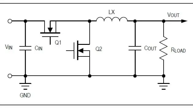
1. How a Synchronous Buck Converter Works
A synchronous buck converter has the following main components:
Basic Operation:
Example Calculation:
Let's say we need to design a 12V to 6V synchronous buck converter supplying 5A of current. Given a switching frequency of 500 kHz and an inductor ripple current of 30% of the load current, we can determine the inductor value:
L=(Vin?Vout)×D/ ΔIL×fsL
Where:
L=(12V?6V)×0.51.5A×500kHz=4μHL
So, a 4μH inductor would be a good choice.
2. Design Considerations
To get the best efficiency and performance, here are some crucial aspects to consider:
(A) Dead Time Management
(B) Proper Gate Drive Circuitry
(C) Inductor Selection
(D) Capacitor Selection
3. Choosing MOSFETs
Selecting the right MOSFETs is critical to an efficient design. Here’s what to look for:
(A) High-Side MOSFET (Q1):
(B) Low-Side MOSFET (Q2):
4. Why Use N-Channel MOSFETs for High-Side Switching?
Advantages of N-Channel MOSFETs:
Lower R_DS(on) → Higher Efficiency
Better Electron Mobility → Faster Switching
Easier to Drive with Bootstrap Circuit
Available in High Voltage Ratings
Why Not P-Channel MOSFETs?
Higher R_DS(on) → More Power Loss
Complex Gate Drive (Requires pulling gate below VIN)
Limited High-Voltage Availability
Example:
If we use an N-Channel MOSFET for a 12V to 6V buck converter, the required gate voltage is:
VGate=Vin+VGS(th)
If V_GS(th) is 5V, then the driver must supply 12V + 5V = 17V, which is achieved using a bootstrap circuit.
N-Channel MOSFETs are the preferred choice due to their efficiency and ease of drive.
5. Additional Design Considerations
(A) Choosing the Right Switching Frequency
(B) Thermal Management
(C) PCB Layout
Conclusion
A synchronous buck converter is a powerful and efficient way to step down voltage in DC-DC applications. By carefully selecting MOSFETs, gate drivers, inductors, and capacitors, you can optimize efficiency and performance.
Using N-Channel MOSFETs for high-side switching, combined with good thermal management and PCB layout, ensures a reliable and high-performance design.