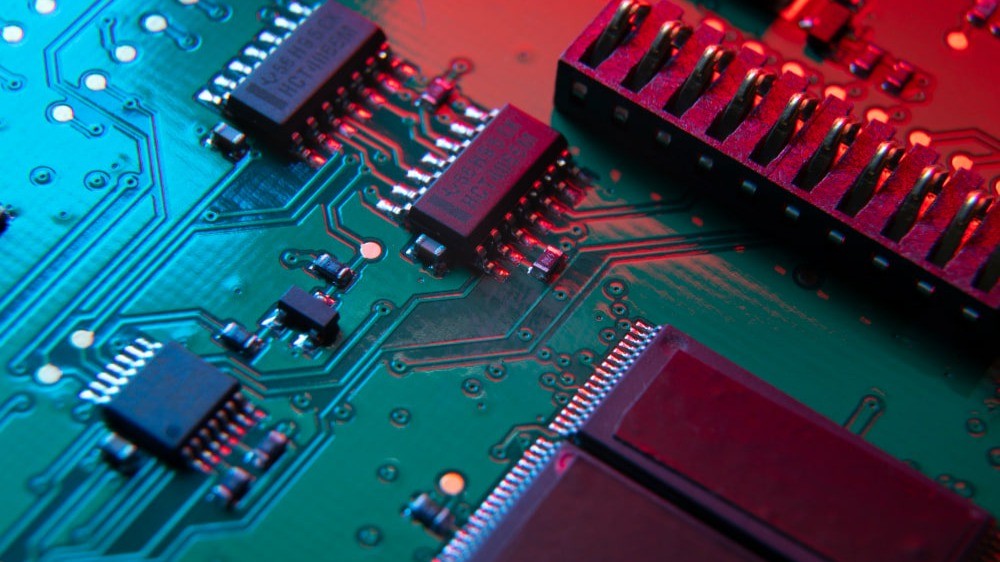
PCB Layout Best practices for Optimal Design
Joseph Ogbonna
Hardware Design Engineer | PCB Design Specialist | Helping Businesses Bring IoT Products to Market | Mentoring the Next Generation of PCB Engineers | Contact Me for Collaboration ??
Introduction
When it comes to designing printed circuit boards (PCBs), a well-planned layout is crucial for ensuring optimal performance, reliability, and manufacturability. Imagine you're designing a PCB for a high-speed communication device. During testing, you notice signal integrity issues and intermittent failures. After troubleshooting, you discover that poorly routed traces and inadequate power supply decoupling are causing the problems. This scenario highlights the importance of a thoughtful layout in preventing such issues.
Whether you're an experienced designer or a beginner, following these best practices will help you create high-quality, reliable PCBs.?
Here are four essential best practices to keep in mind, plus a bonus tip:
1) Keep It Simple and Symmetrical
A simple and symmetrical layout is not only easier to design but also more reliable during manufacturing and debugging. This is especially important in complex PCB designs that have numerous nets and connections. A balanced design with evenly distributed components and traces minimizes the risk of signal integrity issues. Symmetry simplifies the routing process and ensures that the design can be easily modified if changes are necessary. By keeping your layout clean and organized, you’ll reduce potential errors and significantly improve the performance and reliability of your PCB, even in more intricate designs.
2) Minimize Trace Length and Avoid Routing Congestion
The length of your traces directly impacts signal quality, especially in RF designs where trace length can significantly affect performance. Keeping traces short reduces signal delay, attenuation, and electromagnetic radiation, which contributes to a more stable circuit. When traces are kept short, you may not need to worry as much about the critical length of the signal—provided it’s not approaching that threshold. However, it's crucial to always calculate the critical length before making any assumptions to ensure signal integrity. Aim to keep traces under 2-3 inches whenever possible. In cases where longer traces are unavoidable, consider routing techniques like serpentining or meandering to manage length without increasing congestion. Additionally, avoid routing congestion by distributing traces evenly across the board and utilizing multiple layers for more complex designs.
3) Use Decoupling Capacitors Effectively
Decoupling capacitors are essential for filtering out noise and maintaining a stable power supply voltage. To maximize their effectiveness:
领英推荐
4) Avoid Sharp Corners and 90-Degree Traces
In high-speed PCB designs, avoiding sharp corners and 90-degree traces is essential to maintaining signal integrity. Sharp corners and 90-degree angles can cause signal reflections and radiate electromagnetic interference (EMI), leading to potential performance issues. For example, in a high-speed communication PCB, these reflections can distort signals, leading to data corruption or communication errors.
To avoid these issues:
These adjustments help minimize EMI and improve signal integrity, ensuring that your high-speed PCB design functions reliably under various conditions.
Bonus Tip: Follow the 3-2-1 Rule
Adhering to the "3-2-1" rule can further enhance your PCB design:
Biomedical Engineer P.Eng
4 周Hey Joseph. Commenting here as a fan of your content and information but I think these suggestions will lead people down the wrong path in most situations. You say “A balanced design with evenly distributed components and traces minimizes the risk of signal integrity issues”… how so? This doesn’t really mean anything… I think a better tip would be something like: 1. Ensure each routing layer has a continuous return path adjacent to it. Remember signals do not travel down your trace and then back… instead there are two signals that begin at the transmitters output and return pins. These signals are opposite in amplitude and opposite direction. They combine to create an electromagnetic wave that travels through the space between the layers to the receiver. Without a continuous return path your signal will use whatever is nearby to attempt to create a return path… causing noise on your nearby traces and more signal integrity issues.