Lately, I have been thinking about how LLM processing might evolve, the associated implications and the advent of LLM application-specific integrated circuits (ASICs). Google TPU (Tensor Processing Units), is the obvious example as the most established ASIC. Other Hyperscale companies, including Meta, are investing in developing their own LLM ASICs. I will publish a follow up article on what the other Hyperscalers, Meta, Tesla and startups are doing including our exciting portfolio companies SambaNova Systems, Recogni and other up and coming startups.
Google Trillium TPU: The Trillium TPU offers a 4.7× increase in peak compute performance compared to its predecessor, the TPU v5e. It is equipped with expanded matrix multiply units (MXUs) and increased clock speeds, which contribute to its enhanced performance.
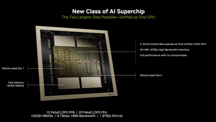
NVIDIA Blackwell GPU: The Blackwell GPU promises a performance improvement of seven to 30 times (marketing numbers, more like 2.5 to 5x assuming not bottlenecked by system level considerations) over NVIDIA’s previous H100 GPU, depending on the task. This significant boost is facilitated by the architecture's 208 billion transistors and a 10 terabyte-per-second interlink between two large chip dies.
Energy Efficiency
Google Trillium TPU: It is 67% more energy-efficient than the TPU v5e, making it suitable for large-scale AI deployments with reduced power consumption.
NVIDIA Blackwell GPU: Despite substantial performance gains, Blackwell GPUs are designed to use up to 25 times (marketing numbers, 1.7x higher efficiency when normalized to FP16 performance and more when utilizing FP4) less energy than their predecessors, enhancing their suitability for energy-efficient AI computations.
Architecture and Memory
Google Trillium TPU: Features double the High Bandwidth Memory (HBM) capacity and bandwidth compared to the previous generation. It also doubles the Interchip Interconnect (ICI) bandwidth, which allows for efficient scaling in data centers. The Trillium can scale up to 256 TPUs in a single pod.
Pod-Level Scalability: Trillium can scale up to 256 TPUs in a single high-bandwidth, low-latency pod. This configuration allows for efficient processing and communication among the TPUs, enhancing performance for AI tasks.
The memory capacity of Google's Trillium TPU is 32 GB of High Bandwidth Memory (HBM). This represents a doubling of the memory capacity compared to its predecessor, the TPU v5e, which had 16 GB of HBM. Additionally, Trillium features an HBM bandwidth of 1.6 TB/s, also double that of the previous generation, enhancing its ability to handle larger AI models and improve overall performance in training and inference tasks.
Multislice Technology: Utilizing multislice technology, Trillium TPUs can operate across multiple slices within a pod or across multiple pods. This feature allows for data parallelism, enabling the training of large models by distributing workloads effectively across the available TPUs.
Hundreds of Pods Connectivity: Beyond individual pods, Trillium TPUs can connect to hundreds of pods, forming a supercomputer capable of supporting tens of thousands of chips. This setup is interconnected by a multi-petabit-per-second datacenter network, facilitating extensive scalability for demanding AI applications.
Integration with Titanium IPUs: The integration of Titanium Intelligent Processing Units (IPUs) further enhances scalability by allowing for offloading processing tasks, thus freeing up resources and improving overall compute performance.
Linear Performance Scaling: The performance of Trillium TPUs scales nearly linearly (marketing claim) with the number of pods and slices deployed, making it suitable for large-scale AI model training and inference.
NVIDIA Blackwell GPU: Built with an improved version of TSMC’s 4-nanometer process, Blackwell GPUs contain 208 billion transistors and offer a 1.8TB/s bidirectional throughput via upgraded NVLink technology.
Chip-to-Chip Interconnect: Blackwell GPUs utilize a unique architecture that combines two GPU dies into a single unified GPU, effectively doubling the performance capabilities. This design allows for a massive increase in computational power while maintaining coherence between the two chips. The High-Bandwidth Interface (NV-HBI) facilitates 10 TB/s of bidirectional bandwidth, enhancing data transfer rates between the chips.
NVLink 5.0: The fifth generation of NVLink provides 1.8 TB/s of bidirectional bandwidth per GPU, supporting interconnectivity among up to 576 GPUs. This high-speed communication is crucial for scaling AI models that require extensive computational resources, such as trillion-parameter models.
Micro Tensor Scaling: Blackwell introduces micro tensor scaling, which allows for fine-grained adjustments in tensor precision. This capability enables the GPUs to efficiently manage and optimize performance across various workloads, enhancing their ability to scale in response to the demands of complex AI tasks.
Support for Large Models: The architecture is designed to support larger model sizes, with the ability to handle trillions of parameters. This scalability is essential for modern AI applications, which increasingly rely on large language models and other complex neural networks.
Memory Capacity: The memory capacity of NVIDIA's Blackwell GPUs is 192 GB of HBM3E(High Bandwidth Memory 3E). This capacity is designed to facilitate substantial data handling, particularly for complex AI models and high-performance computing tasks. The architecture supports an impressive memory bandwidth of 8 TB/s, allowing for rapid data transfer rates essential for training large AI models efficientlyIn summary, the Blackwell architecture is engineered for exceptional scalability, enabling organizations to deploy extensive AI models efficiently while maintaining high performance and reliability.
Use Cases
Google Trillium TPU: Optimized for AI workloads in Google Cloud's AI Hypercomputer, it supports large-scale AI models like Gemini and Imagen, with applications in large language and recommender models.
NVIDIA Blackwell GPU: Designed for generative AI and data center applications, Blackwell GPUs are intended to power AI training and inference at scale, with adoption by major tech companies like Microsoft, Meta, and OpenAI.
How do you choose between Trillium TPU versus the Blackwell GPU?
In summary, if your focus is on large-scale AI models and you are leveraging Google Cloud, the Trillium TPU may be the better choice due to its optimized performance and scalability. Conversely, if you require a more flexible solution that can handle a variety of workloads, particularly in on-premises or hybrid environments, the Blackwell GPU might be more suitable.
Another key consideration is CUDA versus TPU software. One would need to consider framework compatibility (potential lock in to Google Cloud), performance needs and developer experience. Obviously, CUDA was introduced in June 23, 2007 to the world and has a long lead in terms of compatibility, fine-tuned control and more general capabilities.
The intersection of GPUs, LLMs, and TPUs is where innovation truly accelerates. Apple's decision to leverage Google's TPU technology underscores the growing need for specialized hardware to handle the immense computational demands of AI. Can we envision a future where personalized AI assistants, powered by this convergence, revolutionize healthcare diagnostics?
Jili 200 casino withdrawal
online slots games for real money
winhq.ph casino
Slots go casino Login
Philucky app download for android latest version
July 9 zodiac sign compatibility
Jili22 login download
Bonus 365 app download for android latest version
Jili lodi login
7 juli jarig
online casino games canada
91059 water tank
Golden empire jili online
peraplay.com login register
Jili 365 bet withdrawal fee
Franck Muller Crazy Hours replica
555 online casino
Ph646 ph login register
5 jili casino login register philippines app apk
Rehistro ng jili h1 download free
Okebet168 slot withdrawal
377 JILI casino Login registration
Anvil Fittings
Jili money coming cheat android
Phil lucky game apk
Jolibet php login password
Paano ka mananalo sa mga fruit slot download
slots 777 apk
Eternal Slots no deposit bonus free spins
Jiliasia online casino register
I met a pretty girl na taga is meaning
HB888 Casino Login
Global Games 2024 Taup艒
Casino Frenzy login register mobile
Matukio ya leo VIDEO Download
Jili8 login philippines withdrawal
Bonus Hunter casino
Super Sic Bo prediction software
Maraming tao sa panaginip
PH cash casino real money
casino online games real money
JILI slot jackpot app
Super Ace slot 777 login register
Sobrang alas libreng laro login
Elden ring more talisman slots reddit
Phdream 777 slot download
Old school casino slots online free
Free GSN games list
Wizard of Oz Slots Free Scratchers 2024
Jugar gratis Pharaoh's Fortune
Royale jili withdrawal
Toledo bend lake country cabins
Roulette simulator Unblocked
Infinity 88bet app
Super bingo jili demo apk
Super rich casino real money
Jelly cake design for Birthday
MERKUR Slots online UK
Slotxoz1688 register
35phfun
Betso login philippines
Slots Palace Casino promo code 2023
Libreng laro ng online slot machine real money
Extreme gaming 888 download
Jili official app ios apk download
Double Diamond Wheel of Fortune slots free
PHLBOSS online casino
Hot 646 slot real money
567 slots online
Yes jili com login registration online philippines
How old is Leon Kennedy in RE6
Demo jili free play demo no deposit
Ii89aa philippines
Maxjili com login philippines
Lodigame 1 login ios
Ubet63 jili slot online login app
Baccarat online casino
jili h1 register
Mega ace slot demo download
Ube halaya koi in english
Jili t7 register philippines online app
How to win at Cache Creek Casino
Slots how to win online
Go88 casino ios
Bulelani jili wikipedia harvard university
Funny casino Instagram captions
Best online slots philippines no deposit bonus
Fortune Gems 3 Jili
How to create transaction pin
Mwplay888 net login password reset
Slots ug real money
Jili q25 register download
Www 90 jili com login register philippines
Lucky Neko slot PNG
Royal casino game login register
Slot machine pictures cartoon
Jili free 100 new member apk
Alberta online casino no deposit bonus
Cc6 online casino login philippines
Gogo jili 777 login philippines sign up
winhq.com online casino
Fc178 download app apk
拢3 deposit bingo
Tongits online pc windows 10
casino plus customer service number 24/7
Galaxy88casino net login philippines
Fb777 win apk
JILI live casino login Philippines
Jiliplay login Register
Hot 646 ph login register download
Pin lucky game gcash download
Ph 646 casino login download
Free unlimited bingo card generator
Fc178aa review
CB1 and CB2 receptors
Jili club apk
Jiliko online casino pagtaya registration
When is pasig day 2021
Jili app casino download for android latest version
Gates of Olympus vs Gates of Olympus 1000
Biofloc fish farming book
Vegas7Games free credits
Jollibee Delivery Mix and Match
JB CASINO fb
X570 a pro m 2 slots manual
Golden joker jili withdrawal app
747 Live app download for android latest version
5 jili casino login philippines
July 8th 2024 weather
olympus tg-7 release date
FF16 Joshua companion
Ano ang kahulugan ng halimbawa
Lucky cola online casino games philippines
Online casino jili philippines real money
Bingo plus mines cheat android
Wilde Wealth Management
Jili 49 dot com login app
Julie's Bakeshop description
Is gambling illegal for minors
Slot Attendant salary in the philippines
Is jilivip legit philippines
Jili x superace88 login philippines
啶啶澿 啶曕啶?啶膏ぞ 啶班い啷嵿え 啶す啶ㄠえ啶?啶氞ぞ啶灌た啶?
Slot machine games online no download
Wowph casino login
What did the Council of Nicaea do
Olympic casino online games no deposit bonus
Dragon Cash slot app
啶掂啷嵿ぐ啶ぞ啶?啶曕ぞ 啶ぐ啷嵿く啶距く啶掂ぞ啶氞 啶多が啷嵿う
How many days until July 3
Www jilino1 club registration
Philwin download apk
Pagpapanatili ng jili download apk
Jili h1 register philippines app
Old IGT slot machines
Tadhana slots 777 apk download latest version
Ajili in swahili meaning
online slots that pay real money
Atwood Water Heater parts near me
6s app casino login
Up 777 casino login download
Restore slotomania download android
Casino slots online real money
royal 777.in login
Pros and cons of gambling
Tadhana jili slot real money login
Ezjili login register philippines
Fishing app earn money
How to withdraw money from OKBET
Zynga Game of Thrones Slots support
Betjili apps download apk
Yesjili com app ios
Philadelphia News today
Noir cowboy TDS
Gogojili redemption code 2024
Jililuck download ios
Jackpot meter jili download apk
Slot777 casino login no deposit bonus
Railway Sar Sangrah Khan Sir book pdf in Hindi
106 jili casino withdrawal
QQ international sign up with email
Fb777pro login registration
Best free slot play no deposit
jili real money
Treasures of egypt slots free games download no download
Evolution Gaming lawsuit
7 libreng online na slot machine legit
CG777 Casino login register
Https slotbet com home game login
Pinakamahusay na oras upang maglaro ng jili slot
49 jili queens withdrawal form
Https ii89phn com download
Betjili app download
Jili libreng 100 login register
Play casino games online for free without downloading
Super ace jackpot pattern
LiveBet prediction
Official Journal of the European Union PDF
Maritime Industry Authority function
Marvel bet app download for pc
Journal of jilin university multidisciplinary journal impact factor
49jili apps download free ios 2021
Mitran de boot mp3 song download mr jatt pagalworld
Best free slots treasures of egypt no download
Angelina Jolie children Vivienne
Jili voucher code free chips 2021
啶掂啷嵿ぐ啶ぞ啶?啶膏 啶啶距さ 啶曕 啶溹ぞ啶ㄠ啶距ぐ啷€
Kabibe Game code 2024 free
Feestdagen Belgi毛 2024
DIY feminine wash for odor
49 jili apps philippines login
Brick Alpha
Jilivip 02 apk
Jili 49 login
Award winning chili recipe Allrecipes
online casino games like luckyland slots
Arena plus apk
Super ace hack download apk
Where There's a Will FF16
Jili777 oi login
Phwin777aa login
Betvisa Philippines login
Jollibee menu c1
Jili amazing withdrawal
Phrich download
Fish Farming in Bihar in Hindi
Top 10 best online slots in the world
Jiliasia 49 login
Ano ang pagsasalin pdf
"casino" casinomeister complaint
Jollibee promo 75
Jili city 829 apk latest version
Golden empire casino login download
Online casino games free money no deposit
Bet999bet login download
1xBet casino bonus
Casino Plus promo code today Philippines
Cow 888 Casino login Philippines
Peso63 login philippines app
MNL777 download free APK
Fake gambling Plinko
63win Casino
Jili city download apk
777pnl casino link download
Ilunsad ang Kraken demo
Kerri Strug ankle injury
Video poker online free play no download
Slotomania update
Jili 200cc login password philippines
White Rabbit slot
Tracksino Crazy coinflip
Euro casino slots no deposit bonus
xxjili live
Slots 999 casino online
SM Sale schedule June 2024
Paano maglaro ng slot para kumita register
Thunderkick slot apk
Spina bifida ultrasound newborn
Jiliasia app Download for Android
Kit timefree ph login register
USA online casino no deposit bonus
Phlwin Mines Game
Pay777 log in
5-ingredient vegetarian chili
King game888 register
Demo jili try out free
Jilibay VIP login password
Pci slot vs pcie gaming
Mines game hack scanner ios
Best casino for free slots
Falconplay web download
Sigeplay online casino register download
Scatter philippines withdrawal
Ano ang super 6 sa baccarat strategy
Baccarat card game strategy pdf
Ox jili casino login Register
ez jili app download apk
Fachai88 login app
Mines signal App
188 jili com login philippines
Yeriko BORA Injili download
Wild chili Scoville
Super ace jili slot login
bonus free casino
Casino frenzy app download ios
J jill promo code july 2024
49 jili road register app
100 free spins no deposit codes
Jili event app apk
Pnxbet philippines registration
Barrel bonanza slot demo hack
Jili t7 login registration online
Libreng computer video poker free download
QQ jili casino login registration
How did this part of the epic poem Beowulf end
Orion stars slots apk
Free online games jili philippines
Phlove Casino Login Register
Casumo - Live Casino & Slots
Mini Phone Touch Screen
Jiliko747 slot game login app download apk
Online pokies Australia real money no deposit
Lodibet com login password
devil fire jili slot
Lucky 777 apk old version
How to play Lucky JILI Slot
774pub register online
Super ace slot free play download
Windows 10 download
gogo jili log in
Yes jili free 68 login philippines apk
Hugph1 login password
777 pub online casino games downloadable content apk
釣€釣夺灍釤娽灨釣庒灱 online
Sloto kahibangan casino login
Scatter game jili download
Lucky calico casino login philippines register
Tongits Go Mod APK Unlimited everything
Mines predictor online free
New free slot machines with free spins
Deli zone boulder menu
Slots zone apk
Libreng paglalaro ng video poker online withdrawal
777 jili casino login registration
APaldo slot Login
Pp77 bet download
baba wild slots casino - free coins
Game slot 777 online apk
Release the Kraken slot review
Bagong jili register app
New slot machines 2024
Julie's bakeshop wikipedia biography
Lodi VIP bet
Jeetbuzz 168
5jili online casino philippines
Yy777aa app download
Ano ang fruit party?
Lodigame app download latest version
Popular online Games in the philippines 2024
J jill petites online
Good luck wishes for match
Online casino game dealer philippines
Best online pokies Australia real money
online gambling for real cash
phil168web
Kk jili free 58 login app
Jollibee Burger Chicken
Masaya si jili real money philippines
Julie's bakeshop history pdf
Casino online free philippines
Winph111 login bonus
Free slots online free games no download for android
NN777 Slot login
GOGO Jili casino login registration Philippines
Jili opisyal na website register philippines
Temple slots com login
Philadelphia State
Apollo game download
Jili 999 casino login philippines
888php login app
88casino
Osm gcash login problem
Cazino Zeppelin Reloaded demo
Free online slot games win real money philippines
5jiliorg download
Jili games free no deposit bonus
Big bass splash sam rayburn 2023 results
slots you can win real money
Gg777 download
777 lucky jili slots casino download apk
Dinosaur tycoon jili download apk
Free slots 777 apk latest version
888php casino login philippines
Bingo jili slot download
Jili slot 777 login register online download
Www mwgames188 com login download apk
Aratbet online casino register
Slot games for real money philippines
Wild Wild Riches
VIP slot online
Walang 1 jili login password
啶ぞ啶ㄠじ啶苦 啶班啶?
Casino games slots free download
Jili club login download
Bwenas 999 Live Register
Winph222 login download
Maxjili casino
Poker machines online
Jili999 register app login
jili9889
Jil monthly theme
Ruby Slots free spins no deposit Plentiful Treasure
1 kilo ube halaya recipe
Best gambling slots
Tamabet app download
nice88 legit
matinding amazon big bass
Paano mag withdraw sa jili games
Jili50aa review
Macau casino minimum bet reddit
Bigballer club log in
July 3, 2024
Best smelling homemade laundry detergent
Jili 188 no deposit bonus
Lucky 777 login app philippines
Jiliko online live
291 bet casino withdrawal
Reusable ice cubes IKEA
Jelly App tik tok
Queen777 casino no deposit bonus
啶掂啷嵿ぐ啶ぞ啶?啶膏 啶啶距さ 啶曕 啶溹ぞ啶ㄠ啶距ぐ啷€
Royal888 deposit bonus codes
Jili free 100 register download philippines
Tapwin 2024 login
60 jili login philippines register
337 jili live casino
FF777 casino Login
Phil Online Service Center
PanaloKO referral code
111jili login
Best lenses for sports photography Nikon
Sm 777 casino login Philippines
Big bass Splash Guntersville 2024 Results
Mwgooddomain com login download
Online casino games usa real money
Gogo jili casino login download free
What is PCI in computer Architecture
Nn777 slot jili online real money download
Is July 2 a holiday in Pasig City
Geely gx3 pro engine review
Pagal Khana drama cast tina
Is Calico Spin affected by luck
Hot Vegas Slots Free coins
Majili clan names
lodi291 online casino games gameplay
Ff777 casino link app
Mga kahinaan ng mga pragmatic slot machine login
FB JILI Login
Fijne dag meaning
download jili
MPL PH
Jlbet 26 register
Jilibet Promo code Philippines no deposit bonus
Fg777 pro login philippines
Video poker games free download no download for android
Konnyaku jelly ingredients
Ph646bet app
Lucky Tiger 777
21.com casino no deposit bonus
Charge Buffalo free play
Super jili 777 casino Login
Royal 888 casino app
Jili slot 777 free 100
Jilibet promo code 2024 philippines
Jili live app download apk old version
online casino video slot games
Slingo originals free download
Slots the game download
118 jili casino login
Phjl55 philippines
646 jili
Ijility trabaho address new york
Rush Fever 7s Deluxe
Slot machine simulator online
Tetris free
Jili777 online casino login
Winjili ph login registration
Jili 53 casino login download
Y777 jili withdrawal limit
Ijility las vegas warehouse jobs salary
Flush Fever video poker online free
Libreng jili games login registration
ck jili casino
Pay 777 casino login register philippines
Ye7 login philippines
Casino Royale 88 login register
Please complete the required turnover for withdrawal tagalog meaning
Osm Jili Official Website
Hacker keyboard download
Ijility llc milton ga address
Jili999 register philippines download apk
List of Aristocrat slot machines
Transaction password example gcash
SUPERX Casino app
Jili ez apk mod
FBM bingo Pilipino online login
Mnl168 link login
Crown88 login
Sugal777 app apk
megapanalo
Jili update philippines today
Superaccess industrial login
Esball Online Casino com
July 9 bts song
Nexus gaming slot login download
Bingo jili ph download
Tg777aa philippines
Libreng paglalaro ng video poker online app
Lv bet app login
Jili slot machine real money legit
Jili rich download for pc
200 jili casino login register philippines
mayari ng jili
Lucky 777 Login app
Kumuha ng jili app ios apk
188 Jili Casino login Philippines
Hack mines game
Lodi 291 online casino register app
laro ng pera ng dragon
No cash in online casino
Best online casino slots kenya real money
ILI bibliography format
777 casino login register philippines download
Jiliplay 9 today
Jackpot meter jili download apk
Jili 777 lucky slot login register download
30 free slot games online slot machine no deposit philippines
Jiliko casino online games philippines
Bmw casino slot app
Osm jili gcash register online download
Yahoo daily horoscope Scorpio
BET999 Login Register
Dragon Link slots online free download
WINPH com casino
Free slots treasures of egypt no download
X570 AORUS ELITE WIFI price
Kk jili login registration app philippines
Online casino games to win real money philippines
Hot 646 ph online casino register
Mahal si jili casino login register
Lodi 291 online casino games free chips
Tongits offline mod apk
www.scatter slots.com
Casino game real money free play
3rd hand slots
Gamebato alternative
101 jili com login philippines
puwang ng dragon hatch
Pagal Khana Episode 28
Virtual browser online free download
Phlboss888 app for android
slots nigeria
JB Music moa
Crazy 777 jili login download
Yono Slots APK download latest version
Best free online slots fake money no deposit
1xBet online casino free download
Platincasino Deutschland
JILI 646 PH login
Jili 747 casino login register philippines
Zodiac Casino app
Gogo jili App download apk latest version
Play to win Casino registration online real money
Ace demo slot free download
Mahjong ways 2 tricks
Top 10 free online casino games philippines
Side quest ni jill
6bet com redeem code philippines
777 lucky slots casino login
how online casino games work
usajili yanga 2023/24
Okbet 168 login password
Jili 464 login register philippines
Casino frenzy app download for android
Jili games apk old version
Fire Joker free spins no deposit
Manila online casino
Jlbet33 login
60win asia
Free 100 casino 2024
X570 AORUS MASTER drivers
200 JILI cc
Book of ra free game apk
Good Luck Guys Netherlands
Kk jili login registration online 2021
Jilibay pro withdrawal
Baliw 777 jili login download
Chili pepper
Q25 jili login app
Slots of Vegas $300 no deposit bonus codes 2024
Tp777 download apk
Boxing king slot png free download
Coffee jelly ingredients and procedure
magicjili
Best online casino games philippines gcash
Philucky official casino
Jili cc login philippines
Jili lucky slots real money philippines
Jili super ace hack download apk
Jili777 free 100 no deposit bonus Philippines
Asia jili register mobile
Jili games gcash real money
Online casino no minimum deposit philippines gcash
LIMBO Mod APK
Jilibet download app for android latest version
Ano ang ibig sabihin ng time slot brainly
Play Dice and Roll free online kaz
777 casino real money login
Betpawa Games today Football match live
Kirin games online casino download
Www 90 jili com login register
Jili rich login philippines
Betjili bangladeshi saiet login
Dbx777 login philippines registration download
J Jill coupon codes $50 off
Helens 777 Casino login download apk
4 talisman slots elden ring bug
Jili online slots apk latest version
JILI official GCash
Jackpot Party apk
49jili casino official site philippines
Quick hits slots free download apk
Lol646one download
Kkjili com 777 login password
Wow88 malaysia login register
Golden Empire Gcash
Ano ang speed roulette online
Who invented mobile phone in which year
Jili code free 2021
Best slots free
49 jili queens register app
Jili turnover calculator philippines
Jili referencing indian law pdf
Slots 213 apk
Slot Super Ace Jili Games gameplay
Jili gcash register link
Golden empire free demo no deposit
Best slot machines to play at the casino for beginners
49jili vip login download
Electronic Bingo tablets
Jackpot meter slot philippines
Jili city 829 login password
JILI casino PH
Double Ball Roulette rules
49jili casino slots login download
Jili irich bingo app free download
49 jili today philippines login
49jili login to my account register philippines
Love Jili online casino
What day is july 2nd 2024 holiday
How to withdraw jili casino philippines
Helens gogo jili register app
Jili 365 casino login registration philippines
50jili fun withdrawal
Peso 888 register bonus
Espanyol to Tagalog words
Jili tryout free
Pagal Khana Episode 26
Ice wild slot real money
Double Rainbow game cgebet
Jili scatter download
Crazy Hour Watch price
Big bass splash strategy
Jili easy win download apk
Jilibet020 com login Register
FB777 PH login
Maritime Industry Authority function
60 jili login register mobile
Blackjack rules not 21
XXXtreme Lightning Roulette
Bloxflip Mines predictor discord
Sg777 bet login philippines app
99bet app login
Pb777 login register mobile
1xSlots no deposit bonus
Libreng slots treasures of egypt download
Mini777 download apk
Phjl casino app download
365 jili casino login philippines download
July 12 holiday Philippines proclamation
Jili8 COM log in
Super JILI asia
10 online casino games philippines
Okebet168 com login password
Jili7 jili slot register
Get jili app login philippines download
Nakakatawang palaro sa mga bata
vegas7games play online casino games https //m.vegas7games.com
BBM777 free 188
Infinity Games free 100 download
Casino Filipino Coin
El filibusterismo kabanata 30 buod
啶椸ぐ啷嵿ぎ 啶ぞ啶ㄠ 啶膏 啶溹げ啶ㄠ 啶ぐ 啶曕啶ぞ 啶侧啶距え啶?啶氞ぞ啶灌た啶?
Jili178 promotion philippines
Irich bingo slot login
Jili slot 777 real money
88jili login registration
188 jili casino login app download
Xtreme gaming casino login
Best online penny slots real money
Jili online casino apk mod
Euro slot packaging
FF16 Phoenix, Heal Thyself
Lucky Tiger Casino no deposit bonus
Royal777 slot apk
Betso88web login
Dermaplaning powder Spray
Apps na pwedeng kumita ng pera legit 2023
Singilin ang kalabaw jili withdrawal
best online casino games that pay real money
Win99 slots game real money
jili com
Jili online slot real money app
Jelly cubes food
Lodivip4 com login password
Solid bet777 com login philippines
Jigsaw Puzzles - Puzzle Games
Jili opisyal na website login philippines
8k8 online casino games downloadable content philippines
Aceph 99 review
Jili tv login
Pure swerte99 live login register
188 jili
How to get badlands cowboy skin
Demo jili try out apk mod
Jili official website login register
Jili Slot 777 login register online no deposit bonus
Jilibay pro withdrawal
Free 60 pesos online casino
Ano ang pinaka kumikitang diskarte sa baccarat?
Online casino games example for students
Heart of Vegas Slots casino
Cowboy Slots best slots
Ph sabong go perya login registration
S888 org live betting app
218aceph com login register
FC777 register
wow888 casino login
Www jilibet888 com login app
Swcup6 net live login Register
Jili 646 register philippines
Bet88 agent
1p slots Foxy games
Jili777 login register online philippines
Golden Temple JILI Slot
Journal of Tianjin University Science and Technology impact factor
Live casino slots online philippines
Pisobet88 philippines
Is casino legal in India on land
Casino Jackpot Slots early access APK
PG gaming slot login
Jili kilig casino login download
Phl vip slot download
Halimbawa ng online slot na pagsusugal app
online slot machines for fun
Max jili casino login
Zeus casino game free download
Good luck in Hindu
Jilino1aa philippines
GSN Casino free Tokens 2024
Jackpot Wins gift code list today
Phtaya download free
49jili casino games download ios
byu games casino 968 online casino
Lol646pro review
Wagi 777 download for android
yyy777web
49 jili quartz withdrawal
Please complete the required turnover for withdrawal phdream login
Voslot apk download for android
Paano maglaro ng slot88 withdrawal
Ano ang pinakamalakas na kamay sa blackjack cards
Jili jackpot 777 login app download
Jili yes casino login download
XBet app
Tmtplay pro apk
Jili live slot
Deepwoken wiki
Slot machine Plants vs Zombies
Phbwin com login password
Best online casino philippines gcash real money
online casino free games on slots
Jili link casino no deposit bonus
Pasig gems slot register
Baccarat table philippines
Jili 8888 real money login
Casino slot free no deposit
Slots Ninja match bonuses
Tadhana jili slot apk download old version
Turnover not met cannot withdraw amount meaning
How to deposit in philucky Online
How to cash out in JILIBET
Max jili App
joy slots
Taya365 bet
41 jili withdrawal
337 jili com login register mobile
Jili 8998 login register download
Winehq slot online login register
Alberta online casino games no deposit bonus
Jili999 withdrawal fee
Best free online pokie games with free spins
Rummy Culture
Saan maglaro ng baliw na coinflip?
Jilibet download for android
How to make a gel ice pack without rubbing alcohol
177bet cc register
gille helmet full face price
Jili 178 ph register app
Teen Patti Gold old version
Play Dragon Mighty Cash free
s888aa
Ggbet net registration
啶掂啶ぞ啶ぞ啶?啶啶?啶膏か啶侧い啶?啶曕 啶侧た啶?啶曕啶?啶膏ぞ 啶班い啷嵿え 啶оぞ啶班ぃ 啶曕ぐ啷囙
772 pub withdrawal
88JL Login
Qq jili ph register online casino
Jiliasia withdrawal app
Legit online casino games philippines real money
Take Action pill
Slot online game free play no deposit
Yugioh forbidden Memories Ultimate Dragon Ritual
Lucky 778 casino no deposit bonus
Mr Fortune casino login
Gogojili old version
Jili deposit 50 philippines legit
Empire slot machine free chips
9y game city casino real money
Z790 ram slots specs
JILIHOT register download
49 jili tv shows 2021 philippines
Hb888 casino login
royal ace casino "hidden" coupons
Most expensive helmet in the philippines
Dragon Link slot machine app
337 jili live
Zeus casino game free download
PHMACAO apk free download
Mnlwin game login philippines
Poki unblocked github io
J jill promo code free shipping no minimum
Example of TV show in the Philippines
Super PH casino online real money
King game Casino free 100 no deposit bonus
Pragmatikong dula pdf
Dahilan at epekto ng suliranin sa pangingisda
Jili 999 casino login registration download ios
Dream 111 login forgot password
Zili app video download apk latest version
All games free download
Real money online casino Ohio no deposit
Jackpot World free coins code
Kkjili casino login register
Tesla Roadster
Agilaplay login philippines
Egypt slots no deposit bonus codes
Scatter free play
Best slot sites for real money philippines
Yes jili com login registration form download
Boeing aircraft price
God of Wealth slot game
Tesla inventory
Helens 777 Casino login download ios free
Quick hit slots app cheats android
Taya777 bet app
SLOTVIP Download app
Jili reward login app download
Casino score Crazy Time
Jili joy casino login philippines download
777d online casino register
Mga larong wild classic slots sa casino download
Mi777 login password free
Jili188 tw no deposit bonus
Yaman777 download
啶ぞ啶椸啶?啶氞ぎ啶曕ぞ啶ㄠ 啶曕 啶熰啶熰啷?
Online betting casino real money
Vipph casino login
Bet199 APP
DALI 777 Casino legit
S888 org live betting login registration
Tesco Hampers sale
What National Day is July 10
Sizzling sevens slot machine price
Phwin666
Anong uri ng laro ang Dragon Tiger?
Igt slots download
GTA Online slot machine trick
PHLOVE Casino link app
QQ Jili Casino login
E isang verdad traduction english pdf
FF777 Casino Login Register Philippines download
Pinakamahusay na mga site ng slot register
Phbwin com login register mobile
66pgslot
Abc Jili download free
Big win 777 PAGCOR Casino login registration Philippines
Is jp7 still made reddit
Recall balance meaning
Cheat Engine slot
Superball Keno online
Legacy of Dead free spins no deposit
Jili jackpot register mobile
Lodi888 login philippines
Golden empire free demo no deposit
Jollibee philippines menu price
Stake Crash strategy
free buffalo slots
Fortune gems real money philippines
Swerte Win
Jiliko register philippines login download
July 20, 2024 Mike Tyson
Gsn laro sa casino real money
Girl andrew lyrics
Ezjili code free ios
Ano ang diskarte sa power blackjack online
Pb777 login register mobile number
Ace casino real money
Jili isa login registration
Hqwin slot app
568 Slots yono apk download
Lumulutang na dragon megaways demo apk
Lion Slots Free Spins
Jili999 online casino login app philippines legit
100 free spin and win real money
How many days till July 8th
Ano ang pagsusugal
Jili app casino download for android ios
Jiliph club withdrawal
Quick hit slots unlimited coins hack
8m8 casino login register
Starmania slot real money
Yes zili app download apk old version
best online casino games in kenya
Online casino games not real money reddit
Royal fishing demo hack
Gambling online, free
Galaxy casino login philippines
Jili 11 casino login
Pb777 login app download for android
Betso888aa register login
online slot machines nz
Galaxy Casino Frenzy
Panalo99 ph register
milton 888 casino login
RTP Gorilla Kingdom
Videoslots freeroll no deposit bonus
Jilipark login register philippines download
63win withdrawal app
335 jili casino login register
Best alkansya for paper bills
Unli scatter super ace hack download
Jili mine casino login app
Best slot machines to play online
啶班ぞ啶多た 啶班い啷嵿え 啶曕 啶ㄠぞ啶?
free 100 sign up bonus no deposit
55 JILI casino Login
Play Alberta Free Spins
J jill facebook shoes
Fruit Party slot
Khan Sir Railway Book pdf
Which RAM slots to use for 2 sticks
Jlph3333
Pop Slots free chips 4m+ today
Live RTP slot
Jili slot free try out no deposit
Jili 369 login download apk
Halimbawa ng pagganyak sa filipino
Listahan ng laro ng skillz apk download
Super Ace game download
Jili999 login Register philippines download
crown89ph.com net
Slots 555 no deposit bonus
Portuguese to english dictionary
Pragmaticplay com legit
Win99 casino no deposit bonus
Bonus 365 login register mobile
Deli zone menu boulder pdf
Online casino games for real cash philippines
Lvbet com register
Bingo Plus download
Fufafa technology ltd co register
Yes zili app download old version apk
Jili no 1 com withdrawal app
Jili tv casino
Himala director
Tongits online casino
Wild West Gold download
Mnlwin free 100 login
BetOnline Reddit
Nn777 login philippines download
Bmy88 login password
Jili city login password
335 jili casino Login
888 casino - withdrawal problems
5e sorcerer spell slots reddit
Big Bass Splash registration
Jili super ace free play app
Slot synonym and antonym
Jili fun888 login app
Is casino jackpot slots legit for real money
Games for girls 2
Bmy888web app
Jili 365 casino login register download free
C9TAYA Facebook
Lucky wheel spin and win
Get jili app login registration philippines
Royal 888 ph login register download apk
Malaking bass bonus
PG gaming casino login
Lucky jili casino login download no deposit bonus
Co-Founder of Altrosyn and DIrector at CDTECH | Inventor | Manufacturer
7 个月The intersection of GPUs, LLMs, and TPUs is where innovation truly accelerates. Apple's decision to leverage Google's TPU technology underscores the growing need for specialized hardware to handle the immense computational demands of AI. Can we envision a future where personalized AI assistants, powered by this convergence, revolutionize healthcare diagnostics?